U N D E R C O N S T R U C T I O N
Text by Arne Lüker and Karl D. Möller
This page is not working properly with Mozilla Firefox - please use Google-chrome or IE!
This article describes the work done at the National Institute of Research & Development for Technical Physics
in Iaşi, Romania between March 2014 to March 2015.
Surface Plasmon and »radiative« Surface Waves for the NANO to Terahertz Region
1. Preamble
2. Abstract
3. Surface Plasmon and Dispersion Relation
4. Exitation of Surface Plasmon using »Total Reflection« in Prism - Kretschmann Configuration
5. Coupling to Surface Plasmon using a Grating
6. Screen Mode Waves and Surface Plasmon at long wavelengths
7. Conclusion
8. References
This article summarises the theoretical background for a project called:
Development of Surface Wave methods to study the resonances of molecules. Extension of Surface Wave methods to frequencies from Near Infrared to Terahertz region
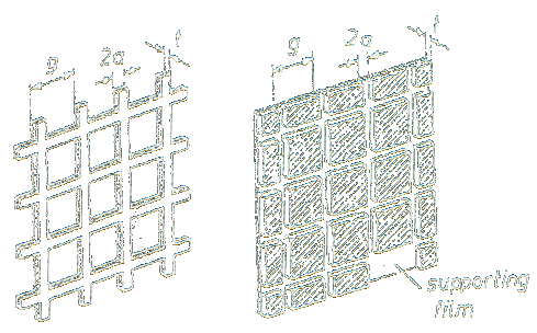 |
| Figure 1: Inductive (left) and capacitive (right) meshes
after R.Ulrich [1]
|
The basic theory and design of inductive screens for the NANO and Short and Mid Infrared region are presented here. An introduction on Surface Plasmons can be found on this webpage:
Programs to do CST simulations were not available at NIRDTP in Iaşi, they were done by K. P. Stewart at NRL (U.S. Naval Research Laboratory), Washington DC.
Proposed work:
- About 2 to 4 Screens should be made for the Short and Mid Infrared.
Then a Surface Wave Method is available for research to use Surface Plasmon at frequencies in Short and Mid Infrared, and Screen Mode Waves in the entire spectral region from NANO to Terahertz frequencies.
- Capacitive screens for reflection measurements in particular for liquids.
Square shaped periodic metal screens may be used to excite »non radiative« surface plasmons in the spectral region of near and mid infrared.
»Radiative« Surface Waves may be excited as resonance modes of metal screens in the total spectral region from visible to Terahertz region,
including the frequency range of characteristic vibrations of molecules.
- Coordinates and Sample position
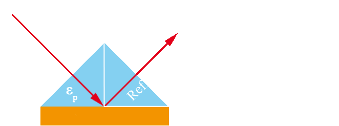
A Surface Plasmon Polariton should propagate on the interface of dielectric and metal. There will be evanescent waves in both media, and samples may be position in the area of the dielectric.
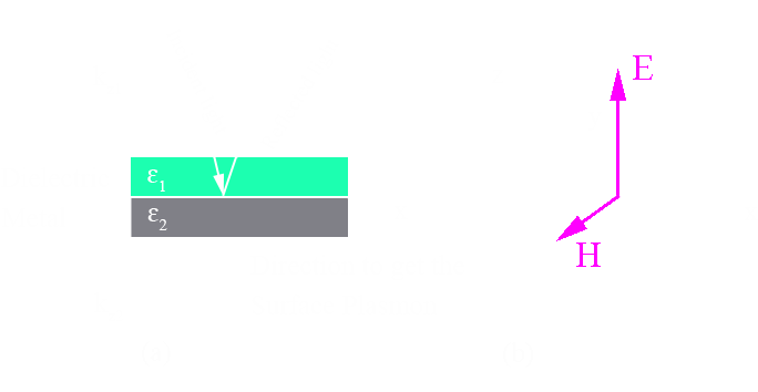 |
| Figure 2: (a) Incident and reflected light. Surface plasmon should be excited at the interface dielectric-metal. (b). Coordinate system (x,y,z) and electric and magnetic vectors.
|
- Dispersion Relations of Surface Plasmon.
Starting with a plane wave solution,
| E |
|
= |
|
E0 ⋅ e (kx x + kz z -w t) |
|
|
|
(Eq.: 1) |
one gets from Maxwell's equations and continuity equations a solution of a wave traveling at the interface in x direction
| kx2+kz12 |
|
= |
|
e1(w/c)2 |
|
|
and |
|
|
kx2+kz22 |
|
= |
|
e2(w/c)2 |
From these equations one gets the dispersion relation:
| ksp |
|
= |
|
(w/c) ⋅ [(e1e2)/(e1+e2)]½ |
|
|
(Eq.: 2) |
w is resonance frequency if Surface Plasmon, e1 is positive, e2 is negative.
- Surface Plasmon and Photon.
The k vector of incident light has the wave vector of a photon, that is
k = (w/c) ⋅ e1½.
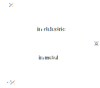 |
| Figure 3: Evanescent waves in z direction at the metal-dielectric interface.
|
The wave vector of a surface plasmon can be written as, ksp = (w/c) ⋅ e1½ ⋅ [e2/(e1+e2)]½.
Since e2 must be negative, one uses metals. Surface Plasmon ksp
is always larger than k of photon of incident light, on account that [e2(e1+e2)]½
is always larger than 1 for large and negative e2.
In w verse k plots, the surface plasmon is always to the right of the »light line«.
As a consequence, a surface plasmon can not be excited from air, that is using e1 = 1.
Since e1 and e2 have in general complex values,
ksp will be complex and as result has a damping factor for propagation. Solution in z direction are evanescent waves,
proportional to e i kx z.
A Surface Plasmon is a »non radiative« wave, always related to evanescent waves in attached materials, while an incident wave is a »radiative« Photons wave, existing in free space.
- Prism and Evanescent Wave.
We look at a prism and make the angle of incidence so large that we get »total internal Reflection« on the base of the prism.
 |
| Figure 4: Prism for Kretschmann Configuration.
|
The k vektors are:
Incident light in air: k = w/c
Component in direction of base line of prism: ka = w/c ⋅ sin q
Component in direction of base line of prism, but inside the prism: kp = w/c ⋅ sin qÖep
We now attach a very small metal film (200nm) to the prism base with contact to the dielectric. The evanescent wave of the prism
penetrates the metal film and a surface Plasmon is excited on the metal-dielectric interface.
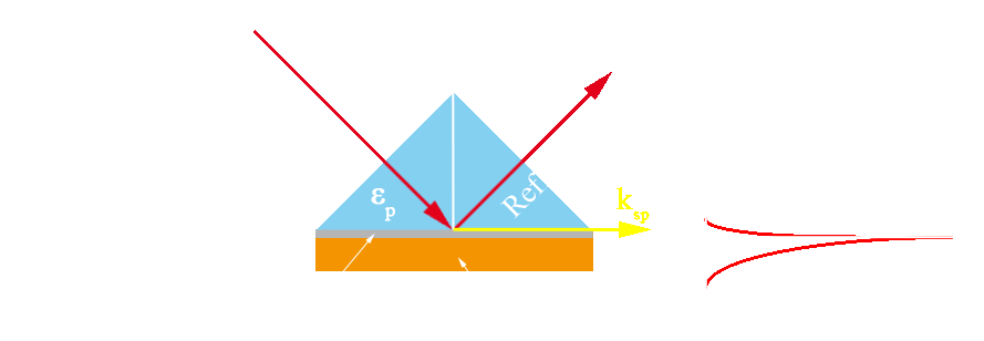 |
| Figure 5: Surface Plasmon and Prism for Kretschmann Configuration.
|
- Matching conditions.
We have for the Surface Plasmon (see Eq.: 2):
| ksp |
|
= |
|
(w/c) ⋅ [(epem)/(ep+em)]½ |
and for the evanescent wave of the prism kp = w/c ⋅ sin qÖep,
where ep is the dielectric constant of the prism and em of the metal film (gray).
For matching we need:
| kp = wi/c ⋅ sin qÖep |
|
should be equal to |
|
ksp = (wsp/c) ⋅ [(epem)/(ep+em)]½ |
By the right chioce of w and for »small tuning« by changing q, one gets
When that is done, we have used in this procedure a »radiative« wave ( incident) to excite a »non radiative« Surface Plasmon.
-
The prism was used to produce an evanescent wave in direction x of interface for excitement of Surface Plasmon.
Instead of a prism, a grating may be used. In Fig.6 a reflection grating is shown. When the periodicity constant is g, the
reciprocal lattice vector is q(2p/g) with q equal +/- integer, presenting the periodicity in frequency space.
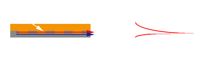 |
Figure 6: (a) Dielectric layer with reflection grating structure. Grating mode (red), Surface Plasmon (blue).
(b) Evanescent waves at dielectric-metal interface.
|
- Matching
If kin = w/c one has for the projection on grating kg = w/c ⋅ sin q Ö ed+ q(2p/g).
To excite a surface plasmon we have to match kg with surface plasmon ksp:
| kg = w/c ⋅ sin q Ö ed+ q(2p/g) |
|
should be equal to |
|
ksp = (wsp/c) ⋅ [(edem)/(ed+em)]½ |
When ed and em are given one chooses (wi/c)
and g, and q for »fine tuning«, such that one has
- Observation.
We consider a surface Plasmon propagating on an interface dielectric ed-Metal as shown in Fig.7.
 |
| Figure 7: (a) Observation of dielectric constant of sample. (b) Observation of absorption
at particular resonance frequency wsp.
|
- Change of Dielectric constant
In Fig.7 (a). Light of frequency w is incident at angle q,
and for one specific set w and q, the surface Plasmon is excited on account that
| k = w/c ⋅ sin q Ö ed |
|
should be equal to |
|
ksp = (wsp/c) ⋅ [(edem)/(ed+em)]½ |
We may consider k(w,q) and ksp(w)
in an w versus k graph for fixed q.
When ep, ed,
and em are given, we get w of surface plasmon
when k(w,q) is equal ksp(w).
A change in q, corresponding to a different ed,
will show up at different wsp in the reflected light at the detector, and from the difference
a change of dielectric constant can be determined.
- Resonance Absorption
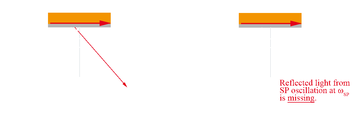
We assume, by changing q, that Surface Plasmon resonance is set at
wsp. When one has a sample with resonance at that frequency, we have resonance interaction. At the reflected light, frequency of light corresponding to Surface Plasmon is missing, indicating resonance absorption at that frequency.
-
Surface Plasmon are »non radiative« waves, used in wavelength range of NANO region and with grating coupling into the near infrared.
When looking at much longer wavelength, from 15 Microns to Terahertz region, one finds that the dispersion relation of Surface Plasmon has about
same value as dispersion relation of surface wave of periodic metal structure, e.g. a square shaped metal screen. We use the same 1-dimensional
presentation as we did for coupling with grating and have then for a Periodic Metal Screen:
| kg = w/c ⋅ sin q + q(2p/g) |
|
and that is almost equal to |
|
ksp = (wsp/c) ⋅ [(edem)/(ed+em)]½, |
of Surface Plasmon for ed = 1 and em
of the order of 102 to 104 and q = 90°.
Surface plasmon are not excited in this spectral region. The surface wave is the resonance mode of the periodic metal structures, and is excited by incident light.
Electrical field of incident wave induces periodic electrical fields at metal structure, using »free electrons« in metal sections for conductivity.
These Screen Mode Waves are »radiative waves«, they exists in free space. Inductive screens are metal plates with holes and are used in transmission.
Inverse structure, called capacitive screens, are used in reflection (Fig. 1). When there are no losses, sum of intensity of transmitted and reflected light is equal to intensity of incident light.
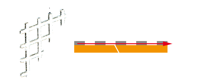 |
| Figure 8: Square shaped inductive metal screen. Periodicity constant g, length of opening L, thickness t.
Optical set-up for transmission, sample layer (orange) may be attached to screen or at separate position.
|
- Surface Wave Modes at long wavelengths region, Bragg Condition
The mode of periodic metal screen will consist of superposition of wave (k1) traveling in one direction and superimposed of the same wave
(k2) traveling in opposite direction. A mode is generated by Bragg scattering, and one has for Bragg condition
| k1 - (-k2) = G |
|
where G is the reciprocal Lattice vector equal |
|
q(2p/g) |
For the wavelength of the mode or standing wave one has
| 2(2p/lres) = q(2p/g) |
|
equal for |
|
q = 1 to 2/lres = 1/g |
|
or |
|
lres = 2g |
Square shaped metal screens, thickness 3-5 Microns, in the spectral region from 15 to 1000 Microns, have for their resonance wavelength the empirical formula
| lres |
|
= |
|
0.75g + 0.5L |
|
|
(Eq.: 5) |
where g is periodicity constant and L length of opening. This kind of screens are commercially available.
- Observation
Resonance Wavelength of Screen Mode Wave depends on dielectric constant of attached layers, and one may find as well resonance absorption.
- Dielectric constant
It has been shown that the resonance wavelength of screens with dielectric layers on both sides, lres,d,
is related to resonance wavelength in air, lres:
| lres,d |
|
= |
|
lres[(e1 + e2)/2]½ |
where e1 and e2 are dielectric constants of dielectric layers on front and backside of screen.
- Resonance Absorption
When using square shaped periodic metal screens one has for transmission spectrum a broad bell shaped curve, see Fig.9. The small peaks at top are »artifacts«
related to incoherent incident light of the spectrometer. There is a range of resonance wavelength at top of transmission curve, useful for the detection of a number of
separate sample resonances within a range of around 20% of top frequency.
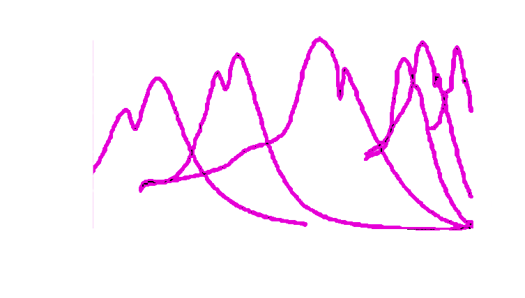 |
| Figure 9: Transmittance Spectrum of set of square shaped metal screens with 2000 to 200 lines per inch. .
|
Square shaped periodic metal screens may be used to excite »non radiative« surface plasmon in spectral region of Near and Mid Infrared.
Square shaped periodic metal screens may be used to excite »radiative« Resonance Screen Mode Waves in total spectral region from visible to
Terahertz Region, including the frequencies of characteristic vibrations of molecules in the infrared spectral region.
- 1. R. Ulrich: Far-infrared properties of metallic mesh and its complementary structure, Infrared Physics, Volume 7, Issue 1, March 1967, Pages 37–55
|
[ back ]